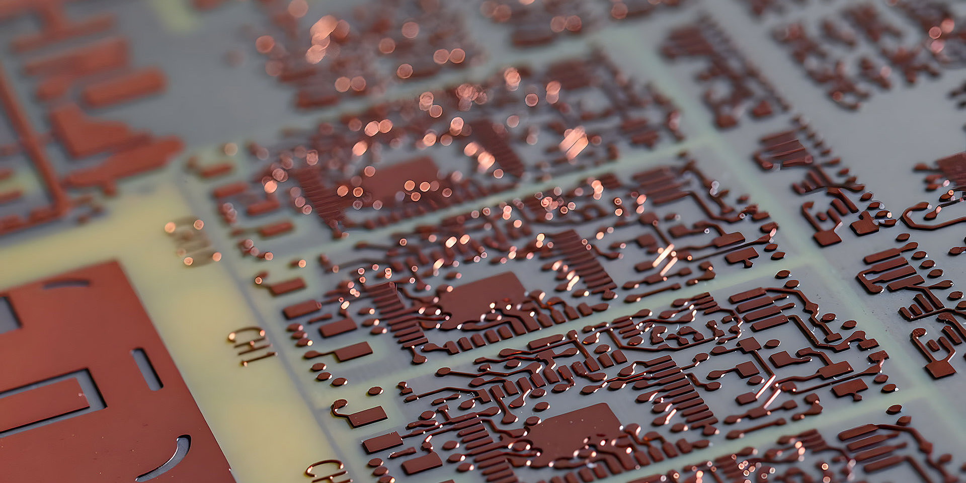
Developed for top performance.
Our broad and almost seamlessly integrated range of products covers the entire spectrum from development and production all the way to market readiness. In addition, our team can provide you with expert support in all related technological and commercial fields.
-
-
Development
-
-
The starting point for your success, to ensure everything runs smoothly from the very beginning.
Our development partners support you during the implementation of your project. You decide, during which development phase you would like to involve us: Drafting of specifications, concept development and evaluation of possible solutions, development, prototyping, integration or testing.
- Drafting of specifications and requirements
- Hardware development
- Firmware development
- Applikations software
- Simulations, e.g. via LTspice
- Housing construction including EMC and insulation
- IR thermography
- Embedded systems (Wifi/Bluetooth)
-
-
-
-
Layout Design
-
-
Our experienced layout specialists are looking forward to tackling the most demanding challenges.
With our many years of experience and the most efficient tools, we realise cost-effective, production-ready and functional designs for your circuit layouts.
- Creation of library elements
- High-speed designs
- All common technologies, including highly complex HDI circuits
- Mentor Graphics: Expedition PCB (layout) / PADS PCB layout and router (layout) / DxDesigner (circuit diagrams) / DesignCapture (circuit diagrams) / PADS Logic (circuit diagrams)
- Altium Designer (circuit diagrams and layouts)
- Converting data from other EDA systems (e.g. Cadence, Zuken, Pulsonix, Eagle)
- Data output via Gerber 274x or ODB++
- Documentation
-
-
-
-
Rigid PCBs
-
-
-
-
From rigid single- and double-sided to multilayer to HDI circuits - we are flexible when it comes to rigid PCBs.
We offer a comprehensive range of technologies and production volumes, from simple-sided PCBs to multilayer and highly complex HDI PCBs.
Single- and double-sided PCBs
Single- and double-sided PCBs still play an important role today. Therefore, we offer you a wide range of products and processes in this field.- Samples, pre-series and series volumes
- Express service from 2AT
- Structures from 75 µm
- Max. PCB size 710 x 1,100 mm
- Max. PCB thickness 10 mm
- Copper thickness up to 1,000 µm
- All common surfaces
- Wide range of base materials
- Solder masks in many common colours
- Carbon printing
Multilayer
Multilayer connections are becoming increasingly popular due to increased component density in technological products and the associated reduction in usable surface area as well as due to the need for facilitating targeted connections to individual components.- Samples, pre-series and series production volumes
- Express service from 3AT
- Up to 44 layers
- Structures from 50 µm
- Max. PCB size 710 x 1,100 mm
- Max. PCB thickness 10 mm
- Copper thickness up to 400 µm
- All common surfaces
- Wide range of base materials
- +/- 3 % impedance control
- Controlled depth milling
- Solder masks in many common colours
- HF circuit boards with all common materials such as Rogers or Panasonic Megtron
HDI
High-density interconnection (HDI) technology has become the standard for multilayer PCBs. It ensures a higher packing density of electronic components and also enables layer-independent layout structures to be implemented using micro-via. Further advantages of HDI are the various routing options for even the smallest BGA pitches and the option to modify parasitic inductance and capacitance effects.- Samples, pre-series and production volumes
- Express service from 4AT
- Up to 44 layers
- Structures from 50 µm
- Copper thickness up to 400 µm
- All common surfaces
- Wide range of base materials
- +/- 3 % impedance control
- Laser-drilled blind/buried vias
- Closed vias according to IPC 4761 Type I to Type VII
- Solder masks in many common colours
- Edge metallisation
- ICT plugging machine for through holes and blind holes
- HF circuit boards with all common materials such as Rogers or Panasonic Megtron
-
-
-
-
Rigid-flex PCBs
-
-
-
-
Rigid-flexible and flexible circuit boards - the ideal solution for every specification.
Due to their inherent design advantages, rigid-flex and flex PCBs allow for sophisticated solutions in even the tightest of spaces.
Rigid-flex PCBs
- Samples, pre-series and series volumes
- Delivery time from 10AT
- Up to 24 layers
- Symmetrical and asymmetrical structures
- Structures from 75 µm
- Max. PCB size 450 x 600 mm
- All common surfaces
- +/- 5 % impedance control
- Laser-drilled blind/buried vias
- Closed vias according to IPC 4761 Type I to Type VII
- Controlled depth milling
- Flexible solder masks and cover foils in different colours
- Wide range of base materials
Flexible PCBs
- Samples, pre-series and series volumes
- Delivery time from 8AT
- Up to 10 layers
- Structures from 75 µm
- Max. PCB size 450 x 600 mm
- All common surfaces
- +/- 5 % impedance control
- Flexible solder masks and cover foils in different colours
- Stiffener in FR4; PI or stainless steel
- Roll to roll
-
-
-
-
Semiflex PCBs
-
-
Semiflex PCBs - the cost-effective alternative.
A cost-effective alternative to rigid-flex PCBs.
- Samples, pre-series and series volumes
- Delivery time from 10AT
- Up to 12 layers
- Structures from 75 µm
- Max. PCB size 710 x 1,100 mm
- Max. PCB thickness 8 mm
- Copper thickness up to 105 µm
- All common surfaces
- +/- 5 % impedance control
- Wide range of base materials
- Laser-drilled blind/buried vias
- Closed vias according to IPC 4761 Type I to Type VII
- Solder masks in many common colours
-
-
-
-
Metal-reinforced PCBs
-
-
Metal-reinforced PCBs - the difference lies in the core.
Copper or aluminium is used for metal-reinforced PCBs, granting them high thermal and electrical conductivity and making them suitable for a wide range of applications.
- Samples, pre-series and series volumes
- Delivery time from 15AT
- Up to 12 layers
- Structures from 100 µm
- Max. PCB thickness 5 mm
- Many years of series production experience with 400 µm Cu on inner layers
- Copper inlays 1 mm to 4 mm
- All common surfaces
- Wide range of base materials
- Laser-drilled blind/buried vias
- Closed vias according to IPC 4761 Type I to Type VII
Aluminium core PCBs
Aluminium core PCBs are characterised by their low weight, high heat resistance and consistent thermal conductivity. They are particularly suitable for use in areas with high heat exposure, such as lighting technology. The automotive industry also relies on the physical properties of aluminum, especially for high-performance engine technology.- Samples, pre-series and series volumes
- Delivery time from 10AT
- Internal or external aluminium
- Up to 12 layers
- Structures from 100 µm
- Max. PCB thickness 5mm
- Aluminium thickness 1 mm to 4 mm
- All common chemical surfaces
- Laser-drilled blind/buried vias
- Different material manufacturers, e.g. Bergquist, EMC, Polytherm
- Different dielectric thicknesses and thermal conductivities
-
-
-
-
Ceramic PCBs
-
-
-
-
Ceramic PCBs - ideal, when things get hot.
Using PCBs on a ceramic substrate basis is ideal for extreme thermal loads. They offer high reliability and long service life in these demanding conditions.
- Samples, pre-series and series volumes
- Delivery time from 15AT
- Up to 10 layers
- Structures from 100 µm
- Standard size 100 mm x 100 mm and 152 mm x 127 mm
- Materials: Aluminium oxide and aluminium nitride
- PCB thickness 0.63 mm to 1mm
- Resistance pressure from 0.1 Ohm to 100 MOhm (1 %)
- Dielectric strength > 15 kv/mm
- Thermal conductivity up to 180 W/mK
- Conductor track pressure in silver (AG), silver palladium (AgPd), palladium gold (PdAu), platinum gold (PtAu), gold (Au)
-
-
-
-
Assembly & Materials Procurement
-
-
-
-
From samples to series production - we are able to supply any volume required.
Materials procurement, assembly, mounting and testing according to client specifications.
- Materials procurement
- SMT, THT and THR assembly
- Assembly of all common types of 01005, BGA, Melf, SOT etc.
- Reflow, wave, selective, manual and iron soldering
- Depaneling with continuous process monitoring
- Press systems with maximum and minimum limit value monitoring
- Optical inspection (AOI)
- Functional testing (FKT)
- In-circuit testing
- Flying probe
-
-
-
-
Cable Assembly
-
-
Cable assembly - so you are always optimally connected.
All types of cable assemblies for your benefit.
- Single strands
- Cable harnesses
- Ribbon cables
- High-voltage connections
- Battery cables
- Assembled control cables
- Overmolded cables and assemblies
- Crimping
- Ultrasonic welding
- Cutting
- Shrinking
- Soldering
- Assembly
- Testing
-
-

Contact
Do you have any questions about our offering?
We are happy to answer them.
D. Kaupke Leiterplatten Service GmbH
Südwestpark 108
90449 Nuremberg
Germany